is the junction capacitance of the diode.
For a typical power diode, the junction capacitance will be around 5pF. For a typical 12:1 turns ratio transformer, the secondary leakage inductance would be around 8nH (very approximate). This would give a ringing voltage across the secondary diode of:
The output capacitor will absorb most of the ringing voltage if it has a low ESR and the PCB track inductance is not too high, but the diode must be able to survive this peak reverse voltage.
Adding the secondary side snubber not only dissipates the energy safely and protects the diode, but reduces the EMI generated by the secondary ringing which can be in the order of tens of MHz. On the other hand, as the ringing frequency is much higher than the switching frequency, it is relatively easy to filter out without incurring a high power dissipation loss.
Typical values for secondary snubber components are 4x the junction capacitance for the capacitor and a resistor value equal to the

term.
In our example, suitable component values for the secondary side diode snubber would be a 20pF capacitor in series with a 40 ohm resistor.
Active clamp and regenerative snubbers
RC snubbers are dissipative circuits: the energy stored in the leakage inductance is diverted by the capacitor and dissipated in the snubber resistor. This consumes between 2%-5% of the total power so the resistor and diodes must be adequately dimensioned to cope with their internal temperature rise.
A more efficient solution is to use active clamping and store the excess energy in a capacitor so that it can be returned to the next cycle. There are two ways to do this; a low-side p-channel clamp in series with the main switch or a high-side n-channel clamp to replace the clamping diode.

Fig.8: Single-ended flyback active clamp configurations: high side and low side configurations
High-side active clamp
The high-side solution shown in figure 8 requires an isolated gate driver but uses a lower cost n-channel MOSFET. Q2 is driven in antiphase to the main power transistor Q1 but with a dead time between cycles to avoid shoot-through.

Fig.9: Single-ended flyback low-side active clamp current flow
Phase 1.Q1 on. Q2 off . Energy is stored in the magnetising and leakage inductances.
Phase 2.Q1 off . Q2 off (dead time). The clamp capacitor starts to absorb the voltage overshoot via the Q2 body diode.
Phase 3.Q1 off . Q2 on. The clamp capacitor charging current is taken over by the FET, reducing the resistance and shorting out the over-voltage spike current into the clamp capacitor. Once the leakage inductance energy has been absorbed,the current in the clamp capacitor reverses and the energy is returned to the Vin capacitor.
Phase 4.Q1 off . Q2 off (dead time). Any remaining energy in the circuit pre-charges the winding capacitance ready for the next cycle.
For higher power applications, an external diode can be placed in parallel with Q2 to reduce the current fl owing through the body diode before the transistor is fully enhanced. The voltage across the high side clamp capacitor is proportional to the duty cycle and Vin:
| Eq. 15 |
 |
Practical Tip: Equation 15 shows that at the lowest Vin, where the duty cycle will be largest, the factor (D/D-1) will approach 1. The voltage across the clamp capacitor will be equal to Vin,
min. At the maximum input voltage, the duty cycle will be low and the factor (D/D-1) will be much less than 1. Therefore, the clamp capacitor does not need to be a high voltage type.

Fig.10: Single-ended flyback high-side clamp current.
Low-side active clamp
The p-channel solution shown in figure 11 is easier to drive but needs a more expensive FET. Q2 is driven in phase with the main power transistor. As the active clamp is p-channel and the main switch is n-channel, Q2 is always off when Q1 is on and vice-versa. A dead-time circuit is not needed as there is no danger of shoot-through, but the different threshold voltages of n-channel and p-channel FETs means that there is a transition period when both transistors are off . This solution has the advantage that both Q1 and Q2 operate in near ZVS.

Fig.11: Single-ended flyback low-side active clamp current flow
Phase 1.Q1 on. Q2 off . Q1 switches on in near-ZVS. Energy is stored in the magnetising and leakage inductances. The voltage across the clamp capacitor is zero.
Phase 2.Q1 off . Q2 off (transition time). The energy stored in the leakage inductance is diverted into low side clamp capacitor by the body diode of Q2 (the body diode is forward biased). The voltage across Q2 stays at one diode drop.
Phase 3a.Q1 off . Q2 on. Q2 switches on in near-ZVS. The clamping capacitor rapidly absorbs the energy stored in the leakage inductance via the low R
DSon impedance of Q2.
Phase 3b.Q1 off . Q2 on. Once the energy in the leakage inductance has been fully dissipated, the current reverses and energy is transferred from the clamp capacitor back into the input capacitor.
Phase 4.Q1 off , Q2 off . The body diode of Q1 holds the voltage across Q1 to one diode drop. Any remaining energy is returned to the input capacitor via this body diode. The voltage across the clamp capacitor is proportional to the duty cycle and Vin:
| Eq. 16 |
 |
Practical Tip:Equation 16 shows that at the highest Vin, where the duty cycle D will be smallest, the factor (1/1-D) will approach 1. The voltage across the clamp capacitor will be equal to Vin
max. At Vin
min. the duty cycle will be large and the factor (1/1-D) will be much higher than 1. Therefore, the clamp capacitor needs to be a high voltage type.
Regenerative clamp
A regenerative snubber can be made using an additional winding on the transformer which has one end tied to ground. The free end injects current into the clamp capacitor to help cancel out the voltage spike created when the switching transistor turns off. (figure 12). The advantage of this circuit is that no active switching is required: the current injection is through steering diodes only.

Fig.12: Single-ended flyback with regenerative snubber using an auxiliary winding tied to ground
Quasi-resonant flyback converter
A Quasi-Resonant (QR) converter can be made to work with most AC/DC topologies, but it is most commonly used as a single-ended flyback. The main difference is that the QR converter PWM timing is dependent on the switch voltage minima rather than on the output voltage alone. A standard flyback controller has a fixed PWM frequency which defines when the next cycle starts, but the QR uses a free-running oscillator with variable off time.
As in the standard flyback topology, the QR topology PWM controller turns on the switch ON to store energy in the transformer core and then turns the switch OFF to allow the energy to be transferred to the secondary. Once the current in the output rectifier diode has fallen to zero, then both input and output windings currents will fall to zero. Any remaining energy in the core will be reflected back into the primary which will start to resonate at a frequency dependent on the primary inductance, Lp, and the lumped drain capacitance, CD, consisting of the sum of the switch capacitance, the coupling capacitance between the windings and any other stray capacitances.
| Eq. 17 |
 |
Resonant frequency of a transformer in QR mode
With a primary inductance of 500μH and a CD value of 1nF, the resonant frequency will be around 225kHz. The voltage across the (open) switch will be the supply voltage superimposed with this resonant oscillation. Choosing to reset the PWM cycle when this voltage is at minimum (valley switching) means that the effective voltage across the switch will be below the supply voltage. This means that the switch now has a much lower turn-on voltage stress and lower turn-on current, both of which will give a measurable increase in efficiency.

Fig.13: QR valley switching
Another advantage of QR operation is that the PWM period timing changes slightly with each cycle depending on the accuracy of the valley detection circuit. This timing jitter flattens out the EMI spectrum and reduces the peak EMI levels. A reduction of 10dB in the conducted interference levels can readily be achieved compared to a conventional flyback circuit. A disadvantage of QR operation is that the PWM frequency is load-dependent and frequency limiting or valley-lockout circuits are needed to cope with no-load conditions.
Half-Bridge Resonant Mode converter
A further development of the QR converter is the fully resonant mode converter design. A Resonant Mode (RM) converter can be made with series resonance, parallel resonance or series parallel resonance (also known as LLC) topologies, but the half-bridge LLC circuit offers particular advantages in resonant mode, so for the sake of simplicity, only this topology will be considered.
The objective of a resonant mode converter is to add sufficient additional capacitance and inductance so that the resonant tank allows Zero Voltage Switching (ZVS). The advantage of ZVS is extremely low losses.
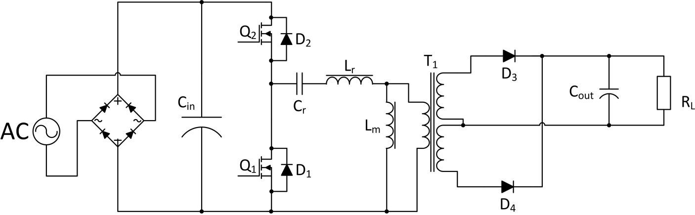
Fig.14: Half-bridge LLC resonant mode topology
This topology has two resonant frequencies. The first being the series resonance tank formed from C
r and L
r and the second the parallel resonance tank formed by C
r and L
m+L
r. Typically, both L
m and L
r are wound side-by-side on the transformer core to reduce the space required. The double resonant frequencies of an LLC converter can be calculated from Equation 17:
| Eq. 18 |
 |
The advantage of the double resonances is that one or the other takes precedence according to load. So while a series resonant circuit has a frequency that increases with reduced load and a parallel resonant circuit has a frequency that increases with increasing load, a well-designed series parallel resonant circuit has a stable frequency over the whole load range. The switching frequency and values of L
r and C
r are chosen so that the primary winding in in continuous resonance and sees an almost perfect sinusoidal waveform. The two half-bridge switches Q1 and Q2 are operated in antiphase. When the FETs are activated, the voltage across them is actually negative. The Gate-Drain voltage is only the internal diode drop and the gate drive current is thus extremely low. As the voltage transitions to positive, the FETs are already ON and start to conduct as the sinusoidal voltage passes through zero.
Combined with the low switching losses and the low transformer losses due to the sinusoidal drive waveform, conversion efficiencies exceeding 95% are readily achievable. Another advantage is that the EMI emissions are extremely low as the entire power train is sinusoidal.
The disadvantages of the LCC converter topology is that the required inductances can be high in order to get a stable resonant frequency with a good Q factor (i.e. low Cr). The converter must also be tuned to operate below the maximum possible gain to allow it start up without problems. Typically a working gain of 80-90% of the maximum is a safe margin.
Additional pulse-mode circuitry may be needed for no-load operation. Although the LLC load range theoretically includes zero load, in practice component tolerances can make the converter unstable with no load.
Finally, the side-by-side transformer construction requires careful design if the creepage and clearance separations required for safety are to be met.
Full-bridge resonant mode converters
Phase-shifted resonant full bridge
A phase-shifted full bridge resonant converter uses a conventional full bridge topology with the addition of a series inductor on the input. The two pairs of switching transistors are driven with two fi xed 50% duty cycle PWM signals which are then phase shifted to control the power delivery. (fi gure 8.15). If the overlap between the two 50% duty PWM signals is low, then only a small amount of energy is transferred across the transformer. If it is high, then full power is transferred. Regulation is thus achieved by shifting the phase of the two PWM signals alone.

Fig.15: Simplified phase-shifted resonant full bridge schematic and the wave forms. The PWM signals are fixed frequency and fixed 50% duty cycle. The blue shaded areas represent the amount of overlap between the two PWM drive signals which controls the amount of power transmission
The advantages of the phase-shifted full bridge topology are that due to the fixed-frequency resonant operation, all of the transistors switch at zero voltage (ZVS) or near zero voltage, so switching losses are very low. The transistor drive circuit is simplified because only two fixed frequency PWM signals which can be very easily generated from flip-flop circuits (50% duty cycle) are needed to drive all four switches. The resonance inductor, L
res, can be omitted if the inherent resonance between the transistor’s C
oss capacitance and transformer leakage inductance is sufficient to ensure ZVS operation. In this case, both D1 and D2 could also be omitted.
Output regulation can be done by either voltage mode, average current or peak current control (by adding a current transformer in series with the high voltage supply), all without changing the basic topology. Peak efficiencies of over 95% are readily achievable with this topology, which makes it especially suitable for higher power AC/DC designs.
The disadvantages of the phase-shifted full bridge topology that the PWM signals must be very precise or have either fi xed dead-bands which reduces efficiency or have variable deadband delays to avoid shoot-through at low loads, making the PWM drive not so simple in practice. Freewheeling (turning on QA + QC or QB + QD simultaneously to circulate the current) is often necessary to clamp the reflected load current and to ensure ZVS conditions which further complicates the drive control and reduces efficiency. Such operating condition-based switching control is often only realizable in practice by microcontrollers running parallel state machines or expensive mixed-signal controllers with internal logic elements.
The supply voltage range is restricted because the efficiency is dependent on resonant ZVS or near-ZVS which is dependent on the square of the supply voltage (eq. 19), so a PFC front end is necessary for a universal mains supply. For higher AC supply voltages (for example, 480VAC), it may be necessary to use cascode switching FETs to meet the V
ds requirements. The resonant inductance needed for ZVS turn-on can be calculated from equation 19:
| Eq. 19 |
 |
The junction capacitance of the two switches in each leg of the full bridge are effectively in parallel during switching, so the individual transistor C
oss values needs to be doubled and added to the measured primary winding capacitance to calculate the resonance capacitance. If the combination of the transformer leakage and magnetizing inductances exceeds L
res,min under worst case conditions, then no external inductor is needed.
Practical Tip: In the equation above, note that doubling the AC supply voltage not only increases the numerator, but also reduces the peak current in the denominator by a squared factor, meaning that a 16 times smaller resonance inductance is needed!
Although the basic concept of the phase-shifted full bridge resonant converter is to use a fi xed-frequency PWM, there are some designs that combine phase-shift control at full load with variable frequency PWM control at low loads to realise high efficiency across the complete load range.
Resonant full bridge
If a series capacitor is added to the circuit shown in figure 15, then a resonant converter with zero voltage switching (ZVS) or zero current switching (ZCS) can be created:

Fig.16: Series resonant full bridge with resonant frequency f
res
Unlike the phase-shifted resonant converter, there is no overlap between the PWM signals with a defined dead time to avoid any chance of an overlap.
Power transfer is controlled by changing the PWM frequency above, equal to or below the resonant frequency of the C
res and L
res restank circuit. This gives three possible modes of operation:

Fig.17: Below resonance, the resonant input current, I
s, leads the PWM switched voltage, V
s. At resonance, I
s is in phase with V
s and above resonance, I
s lags V
s
Mode 1: Below resonance. The input current leads the switched supply voltage, i.e. the impedance is capacitive. The transistors switch in ZCS mode.
Mode 2: At resonance. The input current is in phase with the switched supply voltage, i.e. the impedance is purely resistive. The transistors switch in ZCS mode and the output voltage is at its maximum.
Mode 3: Above resonance. The input current lags the switched supply voltage, i.e. the impedance is inductive. The transistors switch in ZVS mode. The output voltage is at a maximum when the switching frequency is equal to the resonant frequency:
| Eq. 20 |
 |
Where ω is the relative operating angular frequency, ω
sw / ω
res> , and Q is the quality factor:
| Eq. 21 |
 |
Where R
AC represents the transformer load.
The 0.9 factor in the numerator of Eq. 20 comes from a relationship of

which means that at resonance, the output voltage is 0.9V
in (refer to figure 18)
Output power can be reduced by changing the PWM frequency either above or below the resonant frequency, but as ZVS control is optimal for both turn-on and turn-off losses whereas ZCS only helps with turn-off losses, typically an increase in frequency is used to reduce the output power.

Fig.18: Output voltage control by increasing the PWM frequency above resonance
The advantage the variable frequency full bridge resonant controller is high efficiency over a wide load range as the topology remains in resonance from full load down to light load.
The disadvantage is that no-load operation is not possible without losing resonant operation and therefore losing control over the output voltage, so a minimum load is always required.
This drawback can be eliminated by adding an additional resonance capacitor in parallel with the transformer primary winding to make a series-parallel resonant full bridge (figure 19). This topology will stay in resonance from full load down to no-load conditions with good light load efficiency, but requires a PFC front end to provide a stable bus voltage.

Fig.19: Series-parallel resonant full bridge converter
Single-Ended Forward converter
Although the forward converter seems similar to the flyback topology, it functions in a completely different way, relying on continuous transformer action to transfer power from input to output rather than intermittently storing the energy in the magnetic field of the core gap. The input voltage is converted into a regulated output voltage as a function of the turns ratio of the transformer and no gap is needed nor desirable. Figure 20 shows the simplified circuit (refer to the
DC/DC Book of Knowledge for the voltage and current waveforms and explanation of the transfer function).
As the power transfer is continuous over time, we speak of volt-seconds. The volt-seconds during the ON time must not exceed the volt-seconds during the OFF time, otherwise the core will eventually saturate due to a process called flux walking (refer to the DC/DC Book of Knowledge, Chapter 10). This is guaranteed by adding a reset winding that ensures that the core is fully demagnetized at the end of each switching cycle.
As the reset winding ensures that the core fully desaturates at the end of each cycle, the duty cycle can not be higher than 50% maximum, unless a reset winding with a diff erent turns ratio is used. This limits the input voltage range of the converter to typically 2:1, making a universal input AC/DC forward converter more difficult to design than a flyback. Thus AC/DC forward converters are usually used with a PFC front end to give a stable DC bus voltage to work from.

Fig.20: Forward topology (simplified)
As a forward converter transformer has a continuous magnetic core, the magnetic field is more evenly distributed and the associated hysteresis losses and radiated EMI from the concentrated fields across a gap in the flyback topology are avoided.
Other advantages are that the lower peak current reduces winding and diode losses and lead to a lower input ripple is discontinous so high and output ripple current (figure 21). The reset winding transfers excess stored energy back into the PFC capacitor rather than simply having to dissipate the energy in a snubber network. For the same output power, a forward converter will therefore be more efficient than a flyback.

Fig.21: Comparison of forward and flyback (DCM) waveforms. The peak currents in the forward topology are lower and in particular, the output capacitor has a much lower ripple current
The disadvantages of the forward topology are a more complicated transformer construction with an additional resest winding which makes meeting the required creepage and clearance separations more troublesome and an increased component cost as an output inductor, L
out, is needed for each output. If a bipolar (±) output is required where the positive and negative output voltages are complementary, then a transformer style (two inductors sharing the same core) output inductor can be used to save costs. This is not a true transformer but two mutually coupled inductors, so it is important that the windings are bifilar wound to get good coupling and the turns are in the same proportion as the transformer secondaries. This will improve the cross regulation and reduce the output ripple considerably compared to two independent chokes.

Fig.22: Forward converter with bipolar output using a mutually coupled output inductor
If multiple independent outputs are required, then each forward converter output needs an output inductor and capacitor, so in this case, the flyback topology would often be a better choice (but refer also to the current-fed forward converter Section).
As with the flyback topology, snubbers are needed to supress transients to protect the active components. Unlike the flyback, additional voltage transients caused by leakage inductance between the primary and reset windings need to be controlled. In the conventional forward clamp topology with the same number of turns on the primary and reset windings, if the voltage across the switching transistor when it turns off exceeds double the supply voltage, then current will begin to flow in the reset winding. However, this transfer of energy is not instantaneous. The time taken for the current to transfer from the primary to the reset winding is slowed down by the leakage inductance between the primary winding and the reset winding. During this delay, the voltage on the switching transistor will exceed double the supply voltage and can overstress the transistor. The capacitor C
clamp mitigates this overvoltage by providing a low impedance path through the reset winding diode (figure 23).
As the current flows back into the input capacitor, energy is returned into the circuit rather than being simply dissipated through a clamping resistor, so this is an example of a lossless clamp.

Fig.23: Lossless clamp forward converter (simplified)
The required clamping capacitance can be calculated from the following equation (assuming that the primary and reset windings have the same number of turns):
| Eq. 22 |
 |
Where L
p is the primary inductance, N
ps is the primary/secondary turns ratio, V
s is the supply voltage and V
os is the desired maximum overshoot voltage.
As the reset diode has to carry the excess energy transferred via the clamping capacitor, it must be peak current rated > I
load/N
ps. The voltage rating must, of course, be higher than 2V
s.
In addition to the primary side clamp, there is often a need to add snubbers across the switching transistor and secondary diode D2 to control any high frequency ringing that can cause EMI problems.
This is because when Q1 switches on, current starts to flow in the rectifier diode D1, until it has fully charged the output capacitor and now only has to supply the load current. At this point, the voltage across the diode will increase further due to the reflected input voltage transferred by the transformer leakage inductance. As no more current can flow in the load, the current starts to oscillate across the diode D2 junction capacitance. Adding a snubber C
ssn + R
ssn across D2 will absorb this excess energy and damp the ringing (figure 24).

Fig.24: Forward converter with both over-voltage clamp and primary side and secondary side snubbers
Practical Tip:Finding the optimum values for C
ssn and R
ssn can be done by experiment:
- Measure the ringing frequency without a snubber
- Add sufficient capacitance in parallel with D2 until the frequency is halved
- The parasitic capacitance, Cpara is 1/3 of the added capacitance
- The parasitic inductance can be calculated from Equation 23:
| Eq. 23 |
 |
- The snubber resistor should be ideally the same as the characteristic impedance:
| Eq. 24 |
 |
- The power dissipated in the snubber resistor can be calculated from:
| Eq. 25 |
 |
Where f
sw is the operating switching frequency, C
ssn is the secondary snubber capacitor and V
pk is the peak voltage across D2.
If the power dissipation in the snubber resistor is too high, then a compromise may be required to increase the stress on the diode in exchange for reducing the stress on the snubber.
Interleaved Single-Ended Forward
AC/DC forward converters are typically used up to around 200W. Above this power level the high discontinuous primary current cannot be easily handled by increasing the size of the input capacitor bank and by paralleling up the primary switching transistors. Furthermore, the output inductor and capacitor become very bulky.
Synchronous rectification (SR) on the output helps reduce the losses, but using SR makes it difficult to parallel the outputs of two forward converters if more power is required (the SR switching can interfere with the load share current balancing circuit).
One solution to high current, low voltage forward converters is to interleave the power stage using two transformers switched 180° out of phase (figure 25). The additional complexity adds some cost, but this is often balanced out by the reduced size of the input and output capacitors as the ripple currents are significantly reduced (each forward converter stage exhibits a discontinuous RMS ripple current but when added together the overall current is more continuous and approaches DC-see figure 26). Only one input and one output capacitor is needed which also reduces the cost.

Fig.25: Interleaved single-ended dual forward converter topology
The idealized waveform shown below is only valid for a 50% duty cycle. If the duty cycle is changed, then the output currents of the two stages are not perfectly complementary and the ripple currents will increase.
The input capacitor, C
in, will have a ripple current of approximately:
| Eq. 26 |
 |
Where N is the transformer turns ratio and δ is the duty cycle.

Fig.26: Interleaved forward converter waveforms. Note the reduced input and output RMS ripple currents (the output current is almost DC)
Plotted on a graph, figure 27 shows the relationship of normalized input capacitor ripple current to duty cycle. The worst-case input ripple occurs at 0.25 and 0.75 duty cycle.

Fig.27: Input ripple (normalized) vs. duty cycle for an interleaved forward converter
The output ripple current follows a different relationship as in Equation 27:
| Eq. 27 |
 |
Plotted on a graph, figure 28 shows the relationship of the ripple cancellation factor, K(δ), (capacitor ripple current divided by inductor ripple current) to the duty cycle.

Fig.28: Ripple cancellation factor (normalized) vs duty cycle
As can be seen from figures 27 and 28, the interleaved forward converter is most efficient if the duty cycle is very close to 0.5. Therefore, a PFC front end is essential to compensate for input voltage variations while keeping the duty cycle constant.
If more power is needed, then three input power stages and transformers can be wired in parallel with 120°C phase shift. With 0.33 duty cycle, the input and output ripple currents will all superimpose to give a very low combined overall ripple current. And if even more current is needed, then two 180°C interleaved forward converters can be paralleled to deliver 100A. The current balance between these paralleled stages must be very carefully controlled: even a small deviation in the phase current sharing between the stages will increase the ripple currents dramatically.
In practice, some kind of active duty cycle control is needed to compensate for component tolerances, temperature variations and dynamic loads. In addition, each of these paralleled power stages will need their own snubber networks on the primary switch and secondary diodes which will reduce the overall efficiency, especially at low loads. Interleaving the power stages reduces conduction losses (the current paths have lower impedances) but increases the switching losses. At high output currents, conduction losses dominate, but at low output currents, switching losses dominate.
Practical Tip: One technique to improve the efficiency over the whole load range is to shut down one or more parallel phases at low loads. This can add as much as 15% to the low load efficiency by operating the converter as a single-phase forward converter with all of the current flowing through one power stage only. Another saving can be made by switching off the synchronous rectification on the secondary side under low-load conditions and relying on paralleled diodes across the FETs to rectify any residual output current.
Without digital control, such complex feedback mechanisms are impractical, but with a programmable controller it is possible to ensure efficiencies of better than 95% across a very wide load range.
In order to get the best of both worlds and have good efficiency at both very heavy load and light load, a forward converter topology is often preferred for high power, high efficiency designs.
Current-Fed Single-Ended Forward converter
As previously mentioned, a forward converter relies on a storage inductor on the output as ideally no energy is stored or lost in the transformer itself. This means that a multiple output voltage-fed forward converter rapidly becomes very expensive as every output requires its own inductor.
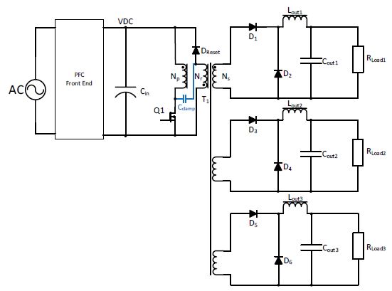
Fig.29: Triple output voltage-fed forward converter with inductors on each output.
The current-fed forward topology adds the inductive storage element on the primary side, making the topology a current converter rather than a voltage converter. This eliminates the necessity of an output inductor and makes multiple outputs more commercially attractive. The disadvantage is that a current source rather than a voltage source is required, typically realized by adding a chopper or buck converter input stage. Output regulation can be achieved by controlling the PWM signal of the input stage only, leaving the forward converter running with a fixed 50% duty cycle (alternatively, the buck converter can be operated with a fixed duty cycle and the forward converter duty cycle modified for regulation). In either case, the topology is insensitive to the rise and fall times so high frequency PWM frequencies can be used to reduce the inductor and transformer sizes.
Current-fed forward converters typically use two-transistor, push-pull or full-bridge topologies (see following sections). This is because the two switches must overlap, so that the current flow through the transformer is continuous and uninterrupted (any break in the current flow would cause destructively high voltages to develop). The primary side inductor limits the current when both switches are on, which also gives the advantage that the topology is inherently short-circuit protected. This is very important for high power applications, as designing a reliable over-current trip with high dynamic current loads is tricky; as the current fed forward topology can tolerate brief short circuit conditions without damage, the over-current trip time can be extended to avoid nuisance tripping in noisy electrical environments.
As an active PFC boost stage is impractical (boost followed by a buck followed by a forward converter), current-fed forward converters are typically used where power factor correction is not an issue, such as in three-phase supplies or where the power is higher than 3kW and the regulations do not apply.
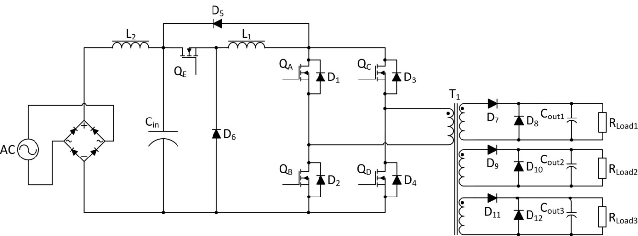
Fig.30: Triple output current-fed full bridge forward converter
L2, C
in, Q
E and D6 form the current source. L1 is the forward primary side storage inductor replacing the inductors on each output. The full bridge configuration avoids the need for a reset winding as long as the duty cycle is ≤50%. D5 clamps and recycles any excess energy back into the input capacitor.
Two-Transistor topologies
Two-Transistor Forward converter

Fig.31: Two-transistor forward topology
Two-transistor (TT) converters are considered one of the most reliable topologies for higher power AC/DC converters. There are several reasons for this:
- The switching transistors have to handle only the maximum input voltage (which is a fixed voltage if a PFC front end is used). Any turn-off switching transients caused by parasitic elements are gated by the fast recovery diodes. This means that the transistors need only be rated for the input voltage plus some headroom, rather than for double the input voltage as in a single-ended switched topology.
- Timing is not critical – as both transistors turn on and off together, there is no requirement for any dead times to avoid shoot-through.
- No snubber networks are needed. Both the residual magnetizing energy and any energy stored in the leakage inductance are transferred back into the PFC capacitor at the end of each cycle by the two diodes. This enhances the efficiency and reduces EMI as excess energy is not dissipated but recycled.
- There is no need for a reset winding, simplifying the construction of the transformer and lowering the cost.
- As the topology is hard switching, no reverse voltages appear across the MOSFETs under any operating condition, so the transistor body diodes are not stressed.
The disadvantages are that ZVS-operation is not possible which limits the operating frequency and that the duty cycle must be kept below 0.5 to allow the transformer time to reset on each cycle. Also, the freewheeling diodes must be the more expensive high voltage fast-acting type.
The disadvantages are that ZVS-operation is not possible which limits the operating frequency and that the duty cycle must be kept below 0.5 to allow the transformer time to reset on each cycle. Also, the freewheeling diodes must be the more expensive high voltage fast-acting type.
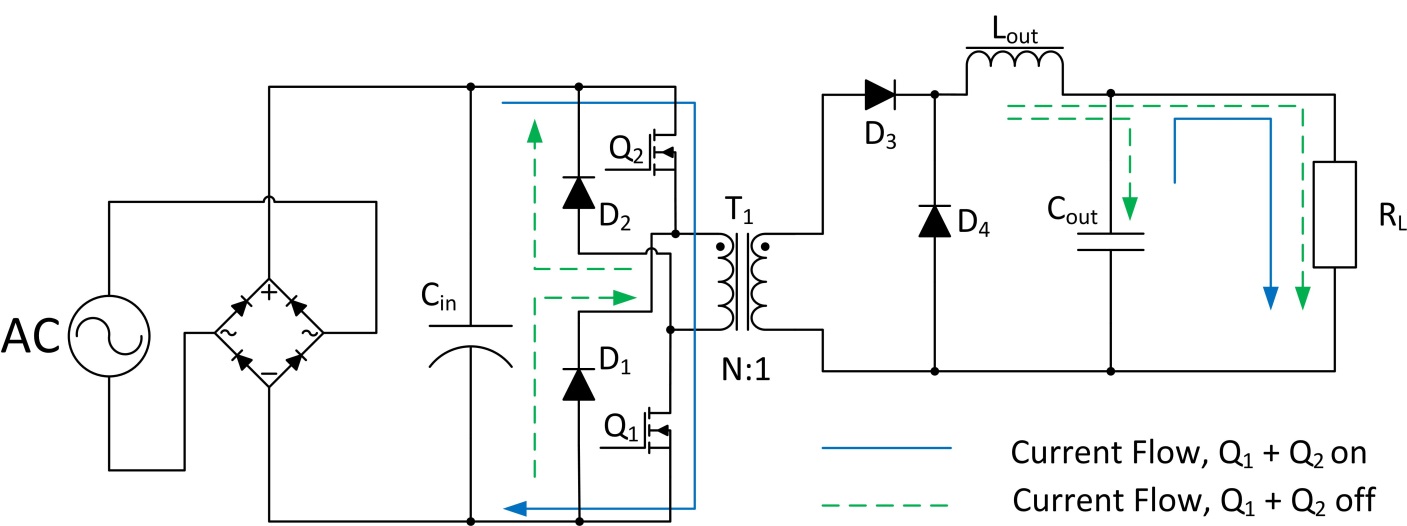
Fig.32: TT-Forward topology CCM current paths with the transistors on (blue) and off (green). Excess energy is returned to the input capacitor at the end of each cycle, so no snubber is required

Fig.33: Current flowing in the switch (I
SW), secondary winding (I
L) and in the primary winding, I
L, mag. As a rule-of-thumb, the peak I
L,mag is chosen to be 1/10th of I
SW,peak
During the first part of the cycle (red), both transistors are on and the freewheeling diodes are biased off . The current through the transistors (I
SW) and in the primary winding (I
PRI) ramps up. During the second half of the cycle, the transistors are turned off (I
SW = 0) and the primary current and magnetizing current ramp down again through the freewheeling diodes back into the input capacitor until the core has been completely demagnetized (green section). The freewheeling diodes then turn off . The time until the next cycle starts (blue section) is the margin needed to ensure that the core is completely reset each cycle. During this time, the primary winding current still continues to ramp down as current is still circulating through the output diode (CCM operation).
Push-Pull Forward converter
The push-pull topology uses a centre-tapped primary and secondary transformer winding and alternately switching transistors. This adds to the complexity of the transformer construction and increases the switching voltage stress on the transistors to 2Vin, but allows four-quadrant use of the magnetic core. In other words, double the power for the same sized transformer core compared to a single-ended forward design.This makes the push-pull topology suitable for AC/DC converters up to 1kW.
However, as the full input current flows through each primary half-winding, they each need to cope with double the current compared to a single-ended design, so they need to be suitably dimensioned to cope.

Fig.34: Push-pull topology and the B-H curve operating area
To avoid core saturation, both transistors need to be switched on for the same time so that the core magnetic flux density swings reliably from B1 to B2 with each cycle and does not “fluxwalk” into saturation. Any imbalance caused by timing errors, winding differences or unequal voltage drop across the output diodes can cause a gradual drift into core saturation as there is no separate core reset mechanism. There are a number of techniques that can be used to avoid or detect impending core saturation: the simplest is to use peak current mode feedback to adjust the Ton times to keep the peak current under control. If voltage mode regulation is required for the application, then an alternative is to add a small air gap to the core so that the core flux density is reduced to manageable levels.
The switching transistors need to cope with at least double Vin (add 20% margin for safety, i.e. 900V rated transistors are needed for a 230VAC input) and be switched with a dead time to avoid shoot-through. This creates severe problems for the output diodes during the deadtimes unless diode snubbers are added.

Fig.35: Primary-side switching waveform (only Q1 shown for simplicity. Q2 is identical but 180° out of phase)

Fig.36: Secondary-side switching waveforms showing the need to add output diode snubbers
Current-Fed Push-Pull Forward converter
An alternative solution that avoids the need for output diode snubbers is to add an inductor on the primary side to make the push-pull current fed. Then the primary side switching waveforms must overlap to keep the current flow continuous:

Fig.37: Current-fed push pull
Making the push-pull current-fed changes the Vin/Vout relationship:
| Eq. 28 |
 |
| Eq. 29 |
 |
Two-Transistor Flyback
The advantages of the two-transistor topology can also be extended to a flyback topology.

Fig.38: Comparison of two-transistor forward (top) and two-transistor flyback (bottom) topologies
As with the TT- forward topology, both transistors in the TT-flyback topology are turned on and off simultaneously. Note that the output winding is reversed with respect to the forward topology. All of the advantages of the two-transistor forward converter also apply to the two-transistor flyback converter:
- The switching transistors have to handle the only the maximum input voltage (which is a fixed voltage if a PFC front end is used) as the overall voltage stress is divided equally over the two transistors and the diodes clamp overshoots to the input voltage.
- Timing is not critical – as both transistors turn on and off together, there is no requirement for any dead times to avoid shoot-through.
- No snubber networks are needed. The leakage inductance energy is gated by the fast recovery diodes and recycled into the input capacitor.
- As the topology is hard switching, no reverse voltages appear across the MOSFETs under any operating condition, so the transistor body diodes are not stressed.
As flyback converters are typically very low-cost applications, the two-transistor flyback is seldom seen despite its inherent advantages, mainly due to the added cost of the additional high-side transistor with its floating gate drive and the need for two expensive fast-acting freewheeling diodes.
The two-transistor flyback can be used in CCM, DCM or CrCM modes, just like the single-ended topology.
In continuous conduction mode, the voltage across each transistor will show a clamped ringing caused by the resonance of the switching transistor’s C
oss capacitance and the primary inductance before stabilizing at half of the combined input and output voltage (figure 39). As this ringing is clamped by the recovery diode and quickly damped by the primary winding resistance, there is no need for a snubber.

Fig.39: Two-transistor flyback in CCM. V
f is the forward voltage drop of the recovery diode, so the maximum voltage stress on each transistor is V
in + V
f. V
ref is the reflected output voltage.
In discontinuous conduction mode, there will be an additional ringing seen on the waveform as the output current falls to zero, again caused by the interaction of the transistor’s output capacitance and the primary winding inductance (figure 40). Again, the recovery diodes clamp the oscillation to limit the voltage stress on the switching transistors.

Fig.40: Two-transistor flyback in DCM
Using paralleled transformers to increase the power
An often-used technique to increase the power of an AC/DC converter is to operate multiple transformers in parallel. This can be done with the forward topology very simply by directly connecting the two transformers to the same power stage and output rectifi ers. Note: the switching is not interleaved but simply paralleled.
The transformers need to be fairly well matched to ensure good power sharing:
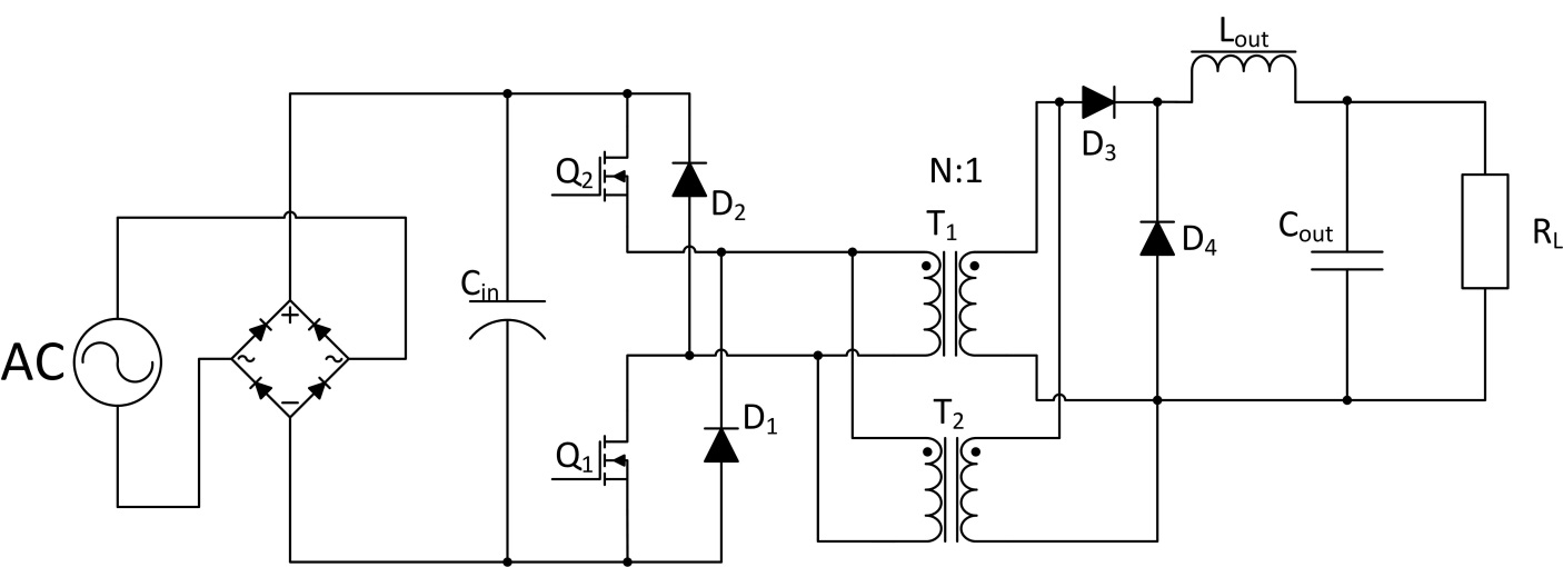
Fig.41: Directly paralleled forward transformers
To allow for production tolerances, it is often better to use separate forward diodes. The current sharing ratio then becomes simply the ratio of the diode forward resistances which are more tightly controlled than the transformer parasitics:
| Eq. 30 |
 |
Practical Tip: As the diode on-resistance is temperature dependent, mount both D1 and D2 close together or on the same heatsink so that they remain thermally matched or, better still, use a double diode with a common cathode:

Fig.42: Paralleled transformers with separate forward diodes
It is also possible to operate transformers in series to share the dissipated power and reduce the core temperatures. This is more commonly called a stacked topology. An elegant solution is to use a capacitive divider to set the centre voltage at half the rectifi ed DC bus voltage. The voltage stress on the switching transistors is then halved. The stacking can be repeated if higher voltages need to be accommodated:
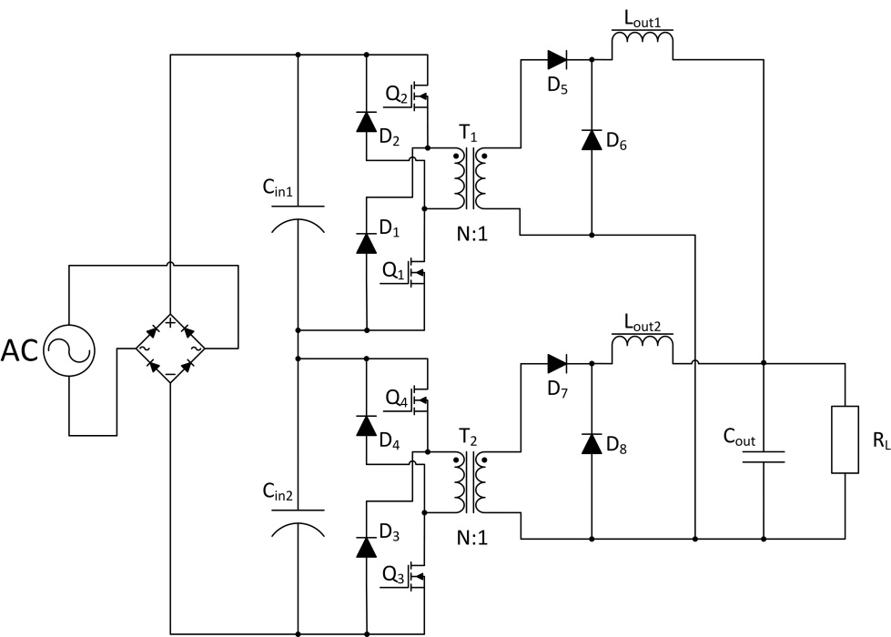
Fig.43: Stacked two-transistors forward converters. Each switching transistor has half the voltage stress of a single stage. If three transformers and capacitors were to be used, then each transistor has a third of the voltage stress
In this interesting example of a stacked interleaved transformer flyback converter*, figure 44, only a single active clamp is required. This variation of a stacked converter uses auxiliary windings on each transformer to improve the power factor by injecting current back into the DC bus voltage (a technique called input current shaping):

Fig.44: Stacked flyback topology with capacitor divider
*Reference: Example is based on “A Single-Phase Single-Stage AC-DC Stacked Flyback Converter with Active Clamp ZVS”, Yuntong Li and Gerry Moschopoulos, Western University, London, Canada.
Published in: 2018 IEEE Applied Power Electronics Conference and Exposition (APEC)
DOI: 10.1109/APEC.2018.8341297
Q1 and Q2 are operated alternately with a suitable dead time between them. During the dead time, Q3 is operated to actively clamp the combined transformer voltage by circulating the current back into clamp capacitor Cclamp. As the clamp current fl ows in both directions, Cclamp must be non-polarized and Q3 switched with a fl oating driver supply:

Fig.45: Stacked converter switching sequence. S3 is the active clamp switching waveform
Stacking or paralleling transformers can increase the power handling if space (especially height) is limited and off ers many opportunities for innovative switching topologies, such as the examples given above. The main disadvantages are increased costs and the difficulty of matching the transformers precisely enough so that parasitic effects (especially leakage inductance diff erences) do not affect the performance. Nevertheless, it is a useful technique in certain situations.
Poly-phase supplies
For higher power AC/DC converters, two or more phases can be used. To full-wave rectify a three-phase input, six diodes are needed:

Fig.46: 3-phase input rectifier
A full-wave three-phase rectifier will generate a peak DC rectified output voltage of:
| Eq. 31 |
 |
| Eq. 32 |
 |
The forward voltage drop across the diode bridge can be assumed to be around 1.2V and can usually be ignored.
| Nominal 3-Phase RMS supply voltage |
Peak rectified DC Voltage (approx.) |
Mean rectified DC Voltage (approx.) |
| 208VAC/60Hz |
486VDC |
464VDC |
| 230VAC/50Hz |
538VDC |
514VDC |
| 277VAC/60Hz |
648VDC |
619VDC |
| 380VAC/50Hz |
889VDC |
849VDC |
| 400VAC/50Hz |
934VDC |
892VDC |
| 415VAC/50Hz |
970VDC |
926VDC |
| 480VAC/60Hz |
1123VDC |
1072VDC |
Table 1: Three-phase full-wave rectified DC voltages
The common point of the three-phase supply can be tied to neutral or to ground, but in many industrial installations earth is preferred. This means that standard single-phase input AC/DC converters cannot be used with phase-to-phase AC power supplies because without a neutral reference point, the voltage between and two phases is much higher (√3 of the phaseto-neutral voltage), for example, a three-phase supply with 230VRMS on each phase has a phase-to-phase voltage of nearly 400VAC.
Even if the standard single-phase input AC/DC converter had an input voltage range that was wide enough to handle the higher input voltage of phase-to-phase operation, there is a separate issue with surge handling capability. A standard single-phase converter needs to withstand at least 1kV peak voltage surges (IEC 61000-4-5, Class 2) in order to meet typical indoor industrial and commercial performance requirements, but three-phase supplies are more often classed as Over Voltage Category III installations with a minimum of 4kV surge withstand capability (IEC 61000-4-5, Class 4). These are minimum levels. More typically, 2kV surge capability for single-phase and 6kV surge capability for poly-phase installations are specified, meaning multiple filter stages are required for compliance.

Fig.47: Example of a three-phase input filter
Practical Tip: The sum of three-phases should be zero volts, so the three phases can be filtered before the rectifier using three X-class capacitors wired to a common point which is then grounded via a Y-class capacitor. As the three-phase supply is assumed to be current limited, only a single fuse after rectification is required for safety compliance.
Three-phase PFC
The PFC circuit cannot be operated from a three-phase supply by simply using a 6-diode input bridge rectifier instead of a 4-diode bridge rectifier because the boost regulation is DCM and the highly discontinuous input current would give a very high THD of ≈30%.
Only if individual inductors on each input are used with CCM control can a three-phase PFC controller with a single switch be implemented:

Fig.48: Three-phase input PFC with CCM control (only one of the phases shown)
The circuit shown above has the advantage of simplicity, but the disadvantage is that the voltage stress on the switching transistor is now very high (realistically, at least a 900V FET would be required).
One solution to the problem of high switching voltage stress is to use an active, three-level rectifier such as the “Vienna” rectifier shown below (there are many variants of this basic topology, but essentially the goal of all of them is to reduce the switching stress on the transistors by using a capacitive divider to halve the supply voltage). The input diodes can be either partly or fully replaced with synchronized switching transistors to increase the efficiency further:

Fig.49: Three-phase Vienna Rectifier topology PFC with alternative half or full active input switching
Despite the reduced input current ripple, a multiple-stage EMC filter is typically still required:

Fig.50: Example of an EMC filtered Vienna topology PFC input stage


 term.
term.


 which means that at resonance, the output voltage is 0.9V
in (refer to figure 18)
which means that at resonance, the output voltage is 0.9V
in (refer to figure 18)


