Moore’s Law, or more accurately his prediction, was that the number of transistors in a complex IC would approximately double every year. Gordon Moore made this statement in a popular magazine in 1965, originally looking only ten years ahead.
He projected that, from around 50 components in an IC in that year, by 1975 there could be 65,000 on a 6 x 6mm die. His forecast proved nearly accurate, with the Intel 8086 released in 1976 featuring 29,000 transistors using a 3.2µm process. Moore later revised his estimate to a doubling every two years. Although the pace of complexity growth has since slowed, TSMC's 2nm process (N2) is on track for volume production in the second half of 2025—an astonishing reduction in feature size by a factor of 1600.
As of 2025, the current record for a consumer/desktop-class microprocessor is held by Apple’s M3 Ultra, which features about 184 billion transistors, achieved with a dual‑die design, fabricated with a 5nm process. This System on a Chip comprises two dies, each with an area of 420mm². Process innovations such as 3D transistors and die stacking have sustained an exponential trend in processing power per mm².

Fig. 1: Moore’s Law in action, showing a selection of milestone processors, their introduction year and their transistor count
Source vs. Load: Why the Load Evolves Faster
When evaluating any system—or collection of systems—in terms of power solutions, power supplies, or analyses related to power consumption, energy efficiency, or energy storage, it is helpful to separate the sources from the loads. At its most basic level, this means distinguishing the power supplies from the end loads that consume the power they provide. Consider the sources and loads as independent black boxes that "communicate" with each other. The figure below illustrates a conceptual breakdown of a system in block diagram form—specifically, a computing or server-like architecture—emphasizing the distinction between typical power sources and loads.

Fig. 3: System Block Diagram Separating SOURCES from LOADS, courtesy of PowerRox [1]
This distinction is particularly important when examining the pace of technological advancement in complex systems composed of numerous components influenced by engineering, manufacturing, and supply chain variables. The trends of exponential improvement, whether transistor count, power density, or
energy efficiency, are more strongly associated with the load side than the source side. Source-side components, typically comprising magnetics, power transistors, and
energy storage, tend to evolve at a slower rate compared to low-voltage semiconductors.
Why Traditional PoL Converter Topologies Can’t Keep Up
In principle, the conversion topologies used in PoL converters have changed little over several decades.
Buck, boost and buck-boost circuits remain standard, still employing a semiconductor switch, diode or synchronous rectifier, inductor, and capacitor, with regulation achieved through pulse-width or frequency modulation. While the core topologies are unchanged, the switches have evolved to exhibit lower static and dynamic losses and to operate at higher frequencies. Inductor core materials have incrementally improved to reduce losses, and capacitor technologies have also advanced. These improvements have collectively increased efficiency, enabling greater power density—allowing PoL converters to become smaller for the same load and temperature rise. However, this progress has not followed Moore’s Law, and power converters continue to occupy a significant portion of board space.
Part of the problem with the size of the PoL converter is that discrete components have traditionally been used on a substrate with little integration. This stems from the simple fact that they are power converters and inevitably dissipate heat, so large components have been necessary to keep temperature rises low. Additionally, the inductor and its core are difficult to fabricate as anything other than a bulky discrete component, and ferrite core technology has only improved in small steps over the decades. This means that a minimum number of coil turns is necessary, which must also be thick enough to withstand higher currents without overheating—resulting in a bulky component. The number of turns required does decrease as switching frequency increases for the same core flux density and output ripple current, but core and PoL converter switching losses also rise, necessitating a larger PoL to dissipate the additional heat. All of this means that, unlike processors, scaling down PoL converters in size tends to directly introduce thermal challenges, limiting overall gains.
Getting Creative While Keeping the Pace
Since load power budgets are decreasing faster than source power availability is increasing, keeping up with Moore’s Law now requires a focus on reducing power budgets rather than simply designing larger power supplies. Intelligent Power Management (IPM) techniques help optimize power distribution and usage in computer systems and data centers [3].
This mindset shift includes:
- Transitioning from always-on to always-available power architectures
- Peak shaving, using energy storage to handle high-power peaks while optimizing steady-state power
- Load shedding/consolidation, turning off unused subsystems to improve power efficiency
- Power allocation optimization, avoiding over-engineering power supplies for worst-case scenarios
Flexible Power Modules for Diverse Applications
Point-of-load converter modules do not follow standard input ranges, and required outputs can range from approximately 0.5V to 3.3V, or up to 5V for legacy designs. Current ratings can also vary widely, from below one amp to tens of amps. The input to a power module may be derived from a regulated bus at 12V, 5V, 3.3V, or sometimes an intermediate value such as 9V. Increasingly, in battery-powered devices, the input may come from a lithium-ion cell—typically around 3.7V, but rising above 4V during charging and falling to 3V or lower when heavily discharged. Alternatively, the input may originate from an unregulated source and vary across a 2:1 range or more.
To support a wide range of applications, RECOM now offers parts in its
RP and
RB series with input ranges as low as 0.85V for boost converters and up to 65V for buck converters. All parts feature adjustable outputs and support applications requiring output voltages from 0.6V to 35V. Current ratings range from 0.5A to 15A. Figure 6 summarizes the available buck converter combinations.

Fig. 6: The wide range of buck power modules available from RECOM, input voltage and output current ratings
Figure 7 similarly shows the range of boost power modules available from RECOM with up to 10A rating. The RBB5-1.5 and
RBB10 parts are buck-boost types where the output can be higher or lower than the input, which is useful for maintaining regulated power from a battery source as it discharges. Boost converters offered up to 1.5A include output overvoltage protection, and all include a true load disconnect function when disabled, which is necessary as there is usually a direct DC path through a boost converter when not switching. All buck and boost converters additionally have over-temperature and output overcurrent protection.

Fig. 7: Boost buck-boost power modules available from RECOM
Has Power Delivery Caught Up with Moore’s Law?
So, have power modules caught up with Moore’s Law? Let’s consider a couple of examples comparing PoL converters with a 24V input and 3.3V output at 4A. Just four years ago, in In 2018, one part was marketed as “leading the advancement of power conversion.” It had a footprint of 33mm × 13.6mm, stood 8.8mm high, and had a volume of 3950mm³. Today, the RECOM
RPX-4.0 has a 5mm × 5.5mm footprint, is 4.1mm high, and occupies just 113mm³—representing a 35-fold increase in power density. Interestingly, the efficiency of both parts is roughly the same; the improvement is entirely due to higher switching frequencies, smaller components, and
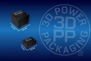
3D Power Packaging® techniques.
Another example is converting 5V to 1.8V at 2A. Older through-hole parts can still be found with a footprint of 14mm x 7.5mm and a height of 10.1mm. In comparison, the RECOM
RPZ-2.0 measures just 3mm x 3mm and 1.1mm high, resulting in a 107-fold increase in power density (Figure 8). The footprint has shrunk by nearly a factor of 12, the RECOM part mounts entirely on one side of the motherboard, and the complications of manual placement and through-hole soldering are eliminated.

Fig. 8: Older technology through-hole 5V to 1.8V/2A PoL converter (left) compared with RECOM RPZ-2.0 (right) (sizes in mm, to scale)
The Value Proposition is Clear
With older open-frame DIP style PoL converters, it was often apparent to users that the same components could be assembled directly on their motherboard, making the value of a purchased module questionable. Even space-saving SIP parts were easily replicated using the same component styles and assembly techniques already employed on the motherboard. However, power modules using 3D power packaging simply cannot be replicated economically with standard motherboard fabrication methods. These modules are now viewed more like standard components—such as resistors or capacitors—that users would never consider building themselves. Their compact size allows them to be fitted easily around or beneath other components, while the highly automated manufacturing processes now employed help reduce costs and improve reliability.
Conclusion
While power solutions may not fully match the pace of Moore’s Law or MEMS scaling, the gap between source and load is narrowing fast. Thanks to intelligent power management, energy storage, and advanced techniques like 3D Power Packaging®, today’s power modules deliver power density far beyond what discrete solutions can offer. These innovations enable compact, efficient, and scalable designs that support modern performance demands. With automation driving down costs and a broad portfolio from RECOM covering everything from handhelds to server boards, module-based solutions are now the clear choice for next-generation electronics.
References
[1] B. Zahnstecher, “Best Practices for Low-Power (IoT/IIoT) Designs: SEPARATING THE SOURCE-SIDE & LOAD-SIDE ANALYSES,” ECCE 2022 Tutorial, Detroit, MI, October 9, 2022
[2] “DC/DC for GaN,” RECOM Blog, Sep 16, 2022, https://recom-power.com/rec-n-dc!sdc-for-gan-225.html (accessed January 23, 2023)
[3] Data Center Facilities Definitions, "Intelligent Power Management (IPM)," TechTarget, https://www.techtarget.com/searchdatacenter/definitions/Data-center-design-and-facilities (accessed February 24, 2023)