
AI Data Center Power Systems: How 800VDC, SiC and GaN Are Changing Power Architecture
Nov 6, 2026

Massive AI data centers cannot afford to waste power, driving a rapid evolution in power system design to maximize efficiency. High-voltage direct current (HVDC) architectures and wide-bandgap (WBG) semiconductors are becoming important elements in the evolution of power distribution and conversion for high-density AI infrastructure.
Table of Contents
- Why Are Legacy Data Center Power Systems Inefficient for AI Racks?
- Transition to High-Voltage DC Bus Architecture
- What Power Components Drive Conversion Efficiency Improvements?
- Wide Bandgap in Detail
- Benefits of and Requirements for SiC and GaN
- Smart Power Equipment and Digital Control
- Future-Proofing Installations
- Summary and RECOM Products
Why Are Legacy Data Center Power Systems Inefficient for AI Racks?
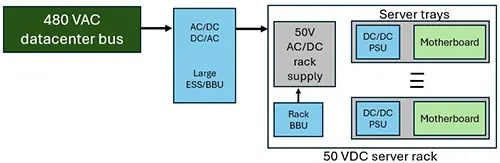
Legacy AC power systems can become increasingly inefficient and difficult to scale as AI rack power rises because power is lost across multiple conversion stages, generating heat while low-voltage, high-current distribution requires substantial conductor cross-sections.
Traditional data center power delivery can rely on substation transformers to convert high-voltage transmission-line AC to a local three-phase AC distribution voltage such as 480VAC in North America or 400/415VAC in other regions. Battery backup units (BBUs) and energy storage systems (ESSs) can introduce additional conversion stages between the facility supply and the rack.
Each conversion stage adds losses and generates heat, while the low-voltage, high-current distribution required further downstream increases conductor requirements. Intermediate and point-of-load supplies then convert the available bus voltage to the lower voltages required by processors, GPUs and other electronic loads.
The industry is developing power architectures for individual AI racks approaching the megawatt range. As an example of the scaling challenge, NVIDIA estimates that delivering 1MW at 54VDC could require up to 200kg (440 pounds) of copper for rack busbars alone (source: https://developer.nvidia.com/blog/nvidia-800-v-hvdc-architecture-will-power-the-next-Generation-of-ai-factoriesNVIDIA 800 VDC Architecture Will Power the Next Generation of AI Factories | NVIDIA Technical Blog) At data center scale, the resulting conductor requirements become a significant design consideration alongside electrical losses, thermal management and available space.
The costs and physical requirements of copper distribution, together with the heat generated by low-voltage, high-current equipment, are directing development efforts toward two key innovation avenues: high-voltage DC distribution to reduce current and conductor requirements, and wide-bandgap semiconductors to improve power conversion performance.
Traditional data center power delivery can rely on substation transformers to convert high-voltage transmission-line AC to a local three-phase AC distribution voltage such as 480VAC in North America or 400/415VAC in other regions. Battery backup units (BBUs) and energy storage systems (ESSs) can introduce additional conversion stages between the facility supply and the rack.
Each conversion stage adds losses and generates heat, while the low-voltage, high-current distribution required further downstream increases conductor requirements. Intermediate and point-of-load supplies then convert the available bus voltage to the lower voltages required by processors, GPUs and other electronic loads.
The industry is developing power architectures for individual AI racks approaching the megawatt range. As an example of the scaling challenge, NVIDIA estimates that delivering 1MW at 54VDC could require up to 200kg (440 pounds) of copper for rack busbars alone (source: https://developer.nvidia.com/blog/nvidia-800-v-hvdc-architecture-will-power-the-next-Generation-of-ai-factoriesNVIDIA 800 VDC Architecture Will Power the Next Generation of AI Factories | NVIDIA Technical Blog) At data center scale, the resulting conductor requirements become a significant design consideration alongside electrical losses, thermal management and available space.
The costs and physical requirements of copper distribution, together with the heat generated by low-voltage, high-current equipment, are directing development efforts toward two key innovation avenues: high-voltage DC distribution to reduce current and conductor requirements, and wide-bandgap semiconductors to improve power conversion performance.
Transition to High-Voltage DC Bus Architecture
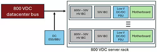
One emerging architecture for high-density AI infrastructure uses an 800VDC distribution bus to reduce current at very high rack power levels. The higher distribution voltage can reduce conductor requirements and I²R losses compared with distributing the same power at lower DC voltages. Battery backup units and energy storage systems are inherently DC-based, creating additional opportunities to integrate energy storage into DC-oriented power architectures with fewer unnecessary conversion steps.
The scale of the difference follows directly from I = P/V: distributing 1MW at 54VDC corresponds to approximately 18.5kA, while the same power at 800VDC corresponds to 1.25kA, before redundancy and derating. This reduction in current is one of the fundamental reasons why higher-voltage distribution becomes attractive as rack power approaches the megawatt range.
The transition does not eliminate downstream voltage conversion. An 800VDC rack bus can feed an intermediate conversion stage to approximately 48VDC, 50VDC or 54VDC, followed by further conversion to 12VDC and ultimately the low voltages required by processors and GPUs. These conversion layers should be distinguished from conventional 1U CRPS/M-CRPS hot-swap server power supplies.
The scale of the difference follows directly from I = P/V: distributing 1MW at 54VDC corresponds to approximately 18.5kA, while the same power at 800VDC corresponds to 1.25kA, before redundancy and derating. This reduction in current is one of the fundamental reasons why higher-voltage distribution becomes attractive as rack power approaches the megawatt range.
The transition does not eliminate downstream voltage conversion. An 800VDC rack bus can feed an intermediate conversion stage to approximately 48VDC, 50VDC or 54VDC, followed by further conversion to 12VDC and ultimately the low voltages required by processors and GPUs. These conversion layers should be distinguished from conventional 1U CRPS/M-CRPS hot-swap server power supplies.
What Power Components Drive Conversion Efficiency Improvements?
Wide-bandgap semiconductors, primarily silicon carbide (SiC) and gallium nitride (GaN), are increasingly used to improve power conversion performance compared with conventional silicon devices in suitable switching applications.
Wide-bandgap materials offer properties that are advantageous for high-efficiency power conversion, including high breakdown field strength and fast switching capability. Depending on the topology and operating conditions, SiC and GaN devices can help reduce switching losses, increase switching frequency and support higher power density. These characteristics are relevant across multiple conversion stages, from high-voltage power conversion to intermediate bus and point-of-load architectures.
Wide-bandgap materials offer properties that are advantageous for high-efficiency power conversion, including high breakdown field strength and fast switching capability. Depending on the topology and operating conditions, SiC and GaN devices can help reduce switching losses, increase switching frequency and support higher power density. These characteristics are relevant across multiple conversion stages, from high-voltage power conversion to intermediate bus and point-of-load architectures.
Wide Bandgap in Detail
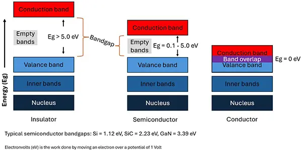
Electrons in materials conduct electricity only when they are in an atom's conduction band. A conductor, such as copper, has overlap between the valence and conduction bands, so electrons move freely. An insulator has a very large gap between the bands, so electrons cannot cross under normal conditions. Semiconductors sit in between: their bandgap is narrow enough for electrons to cross with the addition of energy to the system.
Silicon has a bandgap of about 1.1eV, while SiC (about 3.3eV) and GaN (about 3.4eV) are called wide-bandgap materials because their gaps are roughly three times larger. This wider gap is what gives them a higher breakdown field strength and allows them to operate at higher voltages, temperatures and switching speeds.
The wider bandgap and associated material properties of SiC and GaN enable operation under electrical conditions that can be advantageous in high-frequency and high-voltage power conversion.
In suitable converter topologies, these properties can reduce switching losses and allow operation at higher switching frequencies. Higher frequency can reduce the size of magnetic and passive components, while lower semiconductor losses can reduce cooling requirements. The actual efficiency and power-density improvement depends on the converter topology, voltage levels, switching frequency, thermal design and operating point.
Silicon has a bandgap of about 1.1eV, while SiC (about 3.3eV) and GaN (about 3.4eV) are called wide-bandgap materials because their gaps are roughly three times larger. This wider gap is what gives them a higher breakdown field strength and allows them to operate at higher voltages, temperatures and switching speeds.
The wider bandgap and associated material properties of SiC and GaN enable operation under electrical conditions that can be advantageous in high-frequency and high-voltage power conversion.
In suitable converter topologies, these properties can reduce switching losses and allow operation at higher switching frequencies. Higher frequency can reduce the size of magnetic and passive components, while lower semiconductor losses can reduce cooling requirements. The actual efficiency and power-density improvement depends on the converter topology, voltage levels, switching frequency, thermal design and operating point.
Benefits of and Requirements for SiC and GaN
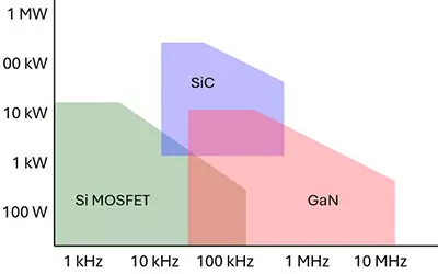
SiC and GaN should not be treated as interchangeable WBG technologies. SiC is particularly relevant to higher-voltage and higher-power conversion stages, while GaN is attractive where very high switching frequency and compact magnetics are priorities. The appropriate device technology therefore depends on the bus voltage, topology, switching frequency, thermal design and required power level.
Higher switching frequencies can also enable larger conversion ratios while reducing the size of magnetic components. In board-level power architectures, for example, an intermediate bus may first be converted from approximately 48VDC or 54VDC to 12VDC before a point-of-load stage generates the much lower voltages required by processors and GPUs. Emerging architectures are also exploring ways to reduce the number of conversion stages while maintaining the transient response required by rapidly changing AI loads. Higher switching frequencies can additionally allow smaller magnetics and faster response to load transients, although these benefits depend on the topology, components and system design.
Higher switching frequencies can also enable larger conversion ratios while reducing the size of magnetic components. In board-level power architectures, for example, an intermediate bus may first be converted from approximately 48VDC or 54VDC to 12VDC before a point-of-load stage generates the much lower voltages required by processors and GPUs. Emerging architectures are also exploring ways to reduce the number of conversion stages while maintaining the transient response required by rapidly changing AI loads. Higher switching frequencies can additionally allow smaller magnetics and faster response to load transients, although these benefits depend on the topology, components and system design.
Smart Power Equipment and Digital Control
Maintenance, uptime requirements and labor efficiencies are driving the transition toward smarter power equipment. Adding a digital interface to monitor and control power devices can make the power supply an active part of the wider power-management system rather than simply a passive conversion component. The open-standard Power Management Bus (PMBus) is an I²C-based communication protocol that can support monitoring, configuration and control of compatible power devices. When implemented as part of a broader power-management system, these capabilities can contribute to functions such as load management, diagnostics and remote fault handling.
Future-Proofing Installations
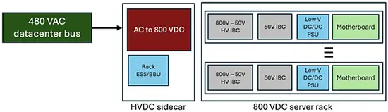
AI data centers are no longer just about raw computing power. Resources such as copper, water for cooling and utility grid capacity are reaching environmental and physical limits. Reducing the thermal, electrical and materials footprint is therefore an important consideration for continued infrastructure scaling. Today's facilities must prepare for future power architectural changes, even if not all downstream systems are ready today.
For future high-density AI installations, the industry is evaluating architectures that integrate energy storage more closely with high-voltage DC distribution. One emerging approach places localized BBU or ESS capacity alongside an 800VDC rack bus, reducing current at high power levels and potentially avoiding some intermediate conversion stages. Such architectures are currently evolving alongside established AC and 48/54VDC power systems rather than replacing them universally.
Higher DC distribution voltage also introduces additional design and safety requirements. An 800VDC system must account for appropriate isolation coordination, creepage and clearance distances, DC-rated connectors and protection, grounding strategy and service procedures. These requirements depend on the actual system topology and applicable standards and cannot be derived from the bus voltage alone.
One transitional architecture uses an 800VDC rack-side distribution bus while retaining the facility's existing AC infrastructure, providing a migration path toward the higher rack power levels expected for future AI systems. Transitioning to this model can require a rack-side power system to convert the facility's existing AC distribution to the high-voltage DC bus. Depending on the system architecture, this equipment can also integrate localized battery backup or energy storage.
For future high-density AI installations, the industry is evaluating architectures that integrate energy storage more closely with high-voltage DC distribution. One emerging approach places localized BBU or ESS capacity alongside an 800VDC rack bus, reducing current at high power levels and potentially avoiding some intermediate conversion stages. Such architectures are currently evolving alongside established AC and 48/54VDC power systems rather than replacing them universally.
Higher DC distribution voltage also introduces additional design and safety requirements. An 800VDC system must account for appropriate isolation coordination, creepage and clearance distances, DC-rated connectors and protection, grounding strategy and service procedures. These requirements depend on the actual system topology and applicable standards and cannot be derived from the bus voltage alone.
One transitional architecture uses an 800VDC rack-side distribution bus while retaining the facility's existing AC infrastructure, providing a migration path toward the higher rack power levels expected for future AI systems. Transitioning to this model can require a rack-side power system to convert the facility's existing AC distribution to the high-voltage DC bus. Depending on the system architecture, this equipment can also integrate localized battery backup or energy storage.
Summary and RECOM Products
Rapidly increasing AI rack power is pushing conventional data center power architectures toward their practical limits in current, conductor size, thermal management and power-conversion efficiency. As rack power continues to increase, higher-voltage DC distribution and wide-bandgap semiconductors are becoming important development paths for the next generation of AI infrastructure.
The resulting architectures will not rely on a single conversion technology. High-voltage distribution, intermediate 48/50/54VDC buses, board-level DC/DC conversion and point-of-load regulation all have distinct roles in delivering power efficiently from the facility to processors and GPUs.
RECOM supports these architectures where board-level power conversion matters most: isolated gate-drive power for SiC and GaN switches, board-level DC/DC conversion, point-of-load regulation and auxiliary power. These solutions complement the broader facility- and rack-level power architecture rather than replacing dedicated CRPS/M-CRPS server power supplies or high-power 800VDC rack power shelves.
The resulting architectures will not rely on a single conversion technology. High-voltage distribution, intermediate 48/50/54VDC buses, board-level DC/DC conversion and point-of-load regulation all have distinct roles in delivering power efficiently from the facility to processors and GPUs.
RECOM supports these architectures where board-level power conversion matters most: isolated gate-drive power for SiC and GaN switches, board-level DC/DC conversion, point-of-load regulation and auxiliary power. These solutions complement the broader facility- and rack-level power architecture rather than replacing dedicated CRPS/M-CRPS server power supplies or high-power 800VDC rack power shelves.
Isolated Gate-Drive Power for SiC and GaN
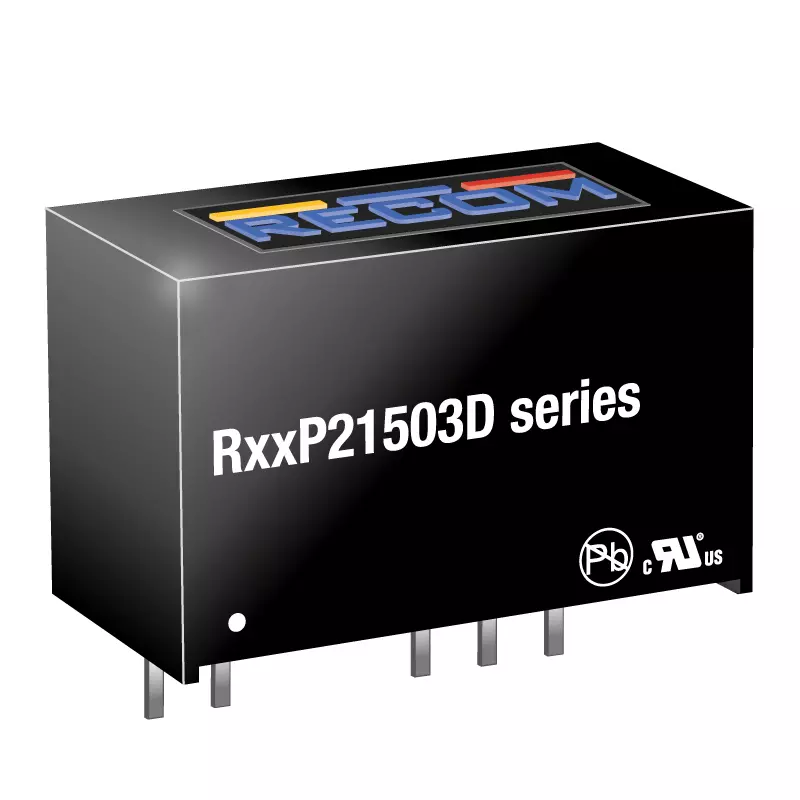
SiC and GaN switches only deliver their efficiency advantage if the gate is driven correctly, and that starts with the isolated gate-drive supply. SiC MOSFETs typically need asymmetric drive voltages such as +15V/−3V or +20V/−5V, while GaN HEMTs typically switch best at around +6V. RECOM offers isolated DC/DC converter families optimized for these requirements, including the RxxP21503 series (+15V/−3V, 6.4kVDC isolation, <10pF isolation capacitance) and RxxP22005 series (+20V/−5V) for SiC MOSFETs, and the RP-xx06, RxxP06, and SMD RA3 series for GaN devices. See the RECOM gate-drive DC/DC converter overview.
Requirements become more demanding as switching edges become faster. Parasitic coupling capacitance across the isolation barrier provides a path for common-mode transient currents, which can contribute to gate disturbance, false triggering and electromagnetic interference. Isolation voltage alone is therefore not sufficient to characterize a gate-drive power supply; coupling capacitance and common-mode transient immunity also need to be considered.
Requirements become more demanding as switching edges become faster. Parasitic coupling capacitance across the isolation barrier provides a path for common-mode transient currents, which can contribute to gate disturbance, false triggering and electromagnetic interference. Isolation voltage alone is therefore not sufficient to characterize a gate-drive power supply; coupling capacitance and common-mode transient immunity also need to be considered.
Board-Level DC/DC Conversion and Point-of-Load
At board level, RECOM DC/DC converters can address intermediate and point-of-load requirements for control, communications, memory, FPGA and auxiliary rails. Different converter families address different input-voltage and current requirements, from 48/54V-related intermediate conversion to compact 12V-fed point-of-load regulation. These modules complement rather than replace specialized GPU multiphase voltage regulators or rack-level power shelves.
Discover how RECOM can support your AI infrastructure design. Explore RECOM's isolated gate-drive converters for SiC and GaN, browse the RECOM DC/DC converter portfolio for board-level and point-of-load power, or contact RECOM's application engineers for help selecting the right solution for your architecture.
Discover how RECOM can support your AI infrastructure design. Explore RECOM's isolated gate-drive converters for SiC and GaN, browse the RECOM DC/DC converter portfolio for board-level and point-of-load power, or contact RECOM's application engineers for help selecting the right solution for your architecture.
Applications


| Series | |||||||
|---|---|---|---|---|---|---|---|
| 1 |

|
RA3
Focus
|
|
| |||
| 2 |

|
RP-xx06
|
|
| |||
| 3 |

|
RxxP06
|
|
| |||
| 4 |
|
RxxP21503
|
|
| |||
| 5 |

|
RxxP22005
|
|
|